









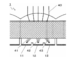
The japanese blog Egami (Click here to read the quirky google translation) found a new Panasonic patent that displays a sort of foveon sensor. The google translation is not so good but as far as I understood that sensor has no Low Pass filter. There is a sort of “photonic crystal” that splits the light into RGB directing the single beams to three different micro sensors. Unlike the Sigma foveon which has three layers placed one under the other the new Panasonic sensor would avoid the light loss typical from foveon sensors (that’s why foveon sucks at high ISO). As usual with patents this sounds very promising. But it is a patent so there is no clue if we will ever see such a sensor in a real camera!
The next patent found by Egami (via Nexthardware) discloses a patented from Olympus that allows a flash sync speed of 1/20.000 of a second! The even more interesting news is that the technology is based on a new electronic shutter system!
85 Responses
A Fovean-type sensor…this is what I have been posting for the last two months that MFT needs to let it compete with the larger sensors from Sony, etc..!!!! This is excellent! Now you’re talking! Is this the revolution? I hope Panasonic can improve the high ISO output of this type of sensor….then we can say “bye, bye” to lacking dynamic range in MFT cameras!!! Time will tell.
Actually this is greatly superior to the “original” Foveon design.
um…I said Fovean-type sensor.
i dont know, it seems like splitting light into 3 pixels instead of one,
increasing resolution by 3 times?
the m43 sensor limitation is everything but resolution, we need improved dynamic range befor anything, i fail to see how this will help
You are completely wrong.
The actual pixel size is the one seen in Foveon sensors, that is, from the light’s “point of view” the 3 subpixels mean just a single pixel – unlike sensors using Bayer grid.
Actually this is the very first sensor design which totally avoids any light loss when filtering the primary colors. The idea is so simple as cannot imagine why nobody has patented it before.
I am more in for the new flash patent, but on the other hand, its for a new electronic shutter only? bummer..
1/20,000th will not be for mechanical shutter….
Okay, n the space of one pixel, they’re going to put three tiny ones?
Sure, it’s not a payer pattern but instead of RGRGRG, BGBGBG, it’s RGBRGBRGBRGB, these are still separate pixels in different places which is exactly what Foveon isn’t.
Honestly, if you wan three pixels in the same space, just use a 3-chip camcorder block where RG&B pixels are indeed stacked p on top of each other. Completely impractical for still cameras but high end video cameras have these.
Also, by tripling the number of sub-pixels, does that means CMOS jello & issues will be compounded by 3?
As for the light loss, it depends on how it is implemented. By the figure it doesn’t seem like a total internal reflection type, so some light will be lost. For the mass market it just depends how they can engineer the thing to be cheap to make — at a nm scale all these small things are difficult to produce.
I am not sure about ‘no light loss’, photonic crystals tends to be very selective for wavelengths. So, from broad spectrum of green you can actually use narrow part of it, just like in conventional bayer arrays with filters. Foveon can detect red to some extent even using green channel, that is way Sigma cameras have troubles with colors.
Nikon has a similar sensor patent from 2009, where they split the light into 3 primary colors thru a prism, and where the sensels are placed side by side.
Correction: it was not in 2009, it was in 2007, and it was not a prism, but a dichronic mirror.
http://www.dpreview.com/news/0708/07080901nikonimagesensor.asp
Actually he’s not completely wrong. Now you have three very small photo sensors per pixel with much less surface area than the Bayer grid both at same megapixel output. You will gain foveon resolution but the iso is bye bye
No, the essence of this patent is different. The resolution is given by the whole cells (one cell per a microlens), not by the ‘subcells’. The idea is to resolve the light rays into colour components by means of the ‘photonic crystal’. These component ‘subrays’ have their own sensors, but they certainly do not add to the resolution, as their source is ‘artificial’ (refraction). The efficiency of the suggested method is supposedly better than that of the Bayer sensor.
How would this compare to one microlens covering the four existing Bayer pixels?
– this would still leave location information in the colour channels which can lead to colour errors (chroma noise, colour aliasing)
– light loss in filters vs. efficiency in splitting the light by colour
> – light loss in filters vs. efficiency in splitting the light by colour
Light loss due to refraction should be much smaller. THAT is the point of the patent, IMO.
Just thinking, would the removal of spatial information from the colour channels (that this patent would provide) also make the correction of spatial lens colour errors (lateral chromatic aberrations) more difficult?
Or would the lack of colour errors (chroma noise etc.) outweigh this?
Exactly!, I was just thinking that!
This sensor design eliminates the light loss due to filtration, and if done right, would restore the one stop difference between APS-C and 4/3 ISO sensitivity/signal-to-noise ratios.
In addition, because signal to noise ratio is improved, you should see a stop more dynamic range, but this will likely also cause base ISO to raise from 200 to 400 unless the gain stage is also adjusted down, which it should be. Overall, this should increase every visible performance statistic, if alignment between subpixels and the prismatic element is very precise.
I wouldn’t expect to see such a sensor for a year or two at least, as photolithography of such a structure would be rather difficult.
+1
Also you get true per pixel RGB sampling… way less chroma noise…. and because you are not filtering away 2/3rs the light from each pixel you might get a 1.5 stop advantage! taking us well into the image quality/iso performance of the best APS-C (nex-5n) and maybe suppasing it because of less color noise… but DR and colour accuracy shold be even better with per pixel RGB sampling! …. bring it!
And yes the amplifacation should be decreased to accomodate this – I would rather it start at ISO50 and end at ISO6400 but with amazing IQ at all ISOs rather than make 2 stops of unusable but impressively numeric ISO at the top end!
6400ISO with an F1.4 and some IS is just about hand held usable in pitch black 🙂
deleted (it was in the wrong place)
“….would restore the one stop difference between APS-C and 4/3 ISO sensitivity/signal-to-noise ratios.
…”
only if they don´t make aps-c sensors out of this….
How so?
actually i can say, I had a micro 4/3 orgasm 10seconds ago.. dreams to come true
TMI
too much information?
too much internet?
touched moved and inspired?
Touch my intestine!
we want thissssss sensor!!!!
So … it has like ‘micro-prisms’ to create rainbows inside sensor… sounds magical 😀
I wonder if that patent will have be used.
Also, Foveon sensors might not be the best in high ISO, but they sure have a nice noise pattern distinct by the near lack of chroma noise.
This patent and the “X” lenses have convinced me at last that it was a right move for me to join m43.
😀 Right
and not only those lenses but also Oly primes are great,+ great compatibility with manual lenses! for me great system
because you have no real clue what all the fuss is about.. what this patent means… right?
this sensor might NEVER see the light.
canon has a zillion patents that never made it into a real product.
don´t be to excited guys.. better use you brains and some caution…
This is not the first sensor patent we see. Though this one looks be more of practical.
Patents are boring – I’d love to start seeing cameras with such sensors soon.
Current Pannay sensor is about 16MP, meaning 16/3 = 5.3MP. Not much, but considering those are true 5.3 million pixels, it’s not that bad.
But I think that the problem they have right here: no marketing department would let a 6MP camera on market.
Sad, especially considering that all my photos land on web/scaled to fit screen (2MP at best).
That’s why the marketing department will call it a 16 Mpx sensor and have the engineers interpolate those extra pixels while, of course, still allowing the user to set the camera to produce image files with only the original pixels. Enthusiasts and pros will have no problems understanding the difference between 5,3 millions of RGB pixels and 4 millions each of R, G, B and G pixels interpolated back to 16 millions.
+1
“Effective” pixels have yet to stop Sigma from marketing their cameras with a 3x multiplier. I doubt that would stop Panasonic. In fact, I doubt that the average consumer understands what a megapixel actually entails, other than “more = better”.
It has, however, stopped Sigma from actually SELLING significant numbers of cameras.
It’s not the low nominal pixel count that scares buyers away. It’s the price tag (and quite a few quirks). And those who can afford a Sigma camera (and can handle its quirks) understand why 4.7 Foveon megapixels outresolve 10.2 Bayer megapixels (as of DPReviews comparison between Sigma DP1 and Nikon D60).
yeh but because the light collection area of each pixel is not reduced it will not be detrimental for panasonic to make a 16mpix X3 (48Mpix) sensor! With better IQ (ISO, DR, colour sampling) than current 16mpix sensor… and as stated no AA filter so you get to keep every bit of that 16mpix resolution… this is BIG if they can manufacture it well!
intel tried to reprogram the brains of pc users that high ghz is not important anymore…at least for a while they tried it in that direction.
so why not brainwash us shooters, at least here it holds true that more mp is not better…
my quad core 2.4ghz is whipping my old 2.6ghz P4…. Intel did have a point…
yes ofcourse but during the p4 era they went almost to the 4ghz…after that they went to new generation architecture and the speed started there at 1,2 ghz…what i meant to say is they reached a limit with the p4 and used a new more efficient setup so they could be excused to user lower ghz…and now they are around 3 ghz again
That was AMD during the “XP” phase. They were right – it’s not the best indicator to go by when comparing different architectures.
the problem with P4 was that Intel was so unable to create an memory controller on the CPU, the other thing why P4 32bit was a so lousy was that amount of L1 cache memory was ridiculously small so that was the bottle neck of the P4.
the last 10 years of cpu development and innovation was driven by AMD, the 1ghz race was the concurred myth of the 90s.
All the great innovation in this field was done by AMD, first cpu over 1000mhz,first memory controller integreted in the cpu, first hybrid cpu 32x-64x, multicore cpu….
Intel is like Canon/Nikon in the world of photography.
Actually, bayer imagers have 1/2 green pixels and 1/4 red & 1/4 blue.
Not an equal amount of each.
http://en.wikipedia.org/wiki/Bayer_filter
and the way any camera counts pixels is hype compared to “old school” film scanning whee a pixel = RG&B information for each dot.
Today these cameras count each R, G or B sensor as a pixel, which is wrong.
http://magazine.creativecow.net/article/the-truth-about-2k-4k-the-future-of-pixels
…but isn’t this the sensor that will be implemented in the upcoming GF7???? 🙂
We can dream!
I wish…you know it is too soon for that. LOL!..but Panasonic does have to come up with something in the sensor dept to compete with it competition!!! At the pace things are moving…the current sensor is totally out-dated.
This is like having 3CCD (http://en.wikipedia.org/wiki/3CCD) the difference being – prism is on every single pixel. As I see it the biggest problem in 3CCD design is size, this may be solution to the problem.
This flash sync time thing would be a real wet daydream for all strobists around errh I have to take a cold shower now.
Yep. Seems more people here are interested in the new sensor, but to me the flash sync speed is the bigger news. I wonder if Panny/Oly realize just how many “strobist” will buy into their system if they can finally get a functional global shutter. It really is a race to see who can get there first. I once bought a Canon G10 simply for the ultrafast flash sync, I’m sure many others will but into m4/3’s if Olympus announces a body that can sync at 1/2000th or better using RF triggers and studio strobes.
Haha, it’s nothing like a foveon sensor :S
potential better… no absorption or blocking by layers… all light gets used… potentialy (depending on prism efficiancy & wavelength division)… by spliting colours then directing each colour to its own sensor… very nice if done well 🙂
Yet another sensor technology that Olympus will not be able to buy into.
Oly will get the G3 Sensor when Panasonic release the new Sensor in some Years.
I hate to say it, but this is a rather obvious idea. I suggested it to the chief architect from a sensor company back in 2000.
Of course it was impossible to fabricate back then, and probably is unmanufacturable at low cost and high yield now.
Nikon has a similar patent that will split the light to three photosites, based on a prism if I remember correctly.
There are two (potential) advantages with systems based on splitting the light:
1. Since the light comes in thru one microlens for each RGB-combination of pixels the deisgn will avoid a lot of antialiasing problems (like Foveon). A side effect of this is that antialisaisng filter isn’t (as) neccessary giving slightly increased resolution.
2. Since a beamsplitter is used in stead of a filter you get a bit more light to the photosites provided the splitter don’t absorb (much) light.
One uknown is how well the beamsplitter split the light close to the wanted RGB-distrobution. If not then they might need complex color calculation simirlar to what Foveon struggles with.
Another potentially more serious problem is that they have to be able to produce it cheaply and with high enough precision.
> Another potentially more serious problem is that they have to be able to produce it cheaply and with high enough precision.
*looks at the price of SD1*
Why do you think it has to be cheap?
If it works perfectly then it will have an significant advantage over Bayer, slightly higher resolution and the photosites may get as much as double the light (equivalent to a full stop), or some other combination of more resoultion and nore ligt to the sensor.
This might be enough (provided nobody else do it) to equialize the difference to APS-C, maybe even a little more.
It’s usually extremely difficult to get the full theoretical advantage from any design so the best I’d expect is APS-C performance which mean that Panasonic should be able to produce it as cheaply to be competititve.
Btw, I’ve no idea why SD1 is so expensive. It might be sensor cost and if so then I don’t understand why Sigma bother at all. I’m sure Panasonic wouldn’t if the saw that the sensor would be to costly to produce.
Well I maybe dense but as shown the crystal splits the light and beams it to 3 locations on the same plane. Why can’t you just put filters in those 3 locations why would you need the crystal? Is it that it’s easier to split the light than create filters at that scale? I ask because one of the advantages of the foveon was those sites were stacked on top of each other and relied on the light penetrating to the stacked layers right???
the filter over each area effectively reduces the light to each sensor down to 1/3rd…. with the prism approach all the light above 3 sensor locations is kept but just diverted to the appropriat sensor location… in effect 3 times better performace than traditional approach.
I think I get it now. Though I still see hurdles I see it could have great promise. Well of course if it’s real good maybe they’ll copy Sigmas marketing example and sell it for $5000 : )
This sensor is great. Panasonic with their old 3CCD Camcorders know how to use beam spliters to get the Colours. The noise was low and the resolution was great.
The biggest problem with this design will be the corners and edges. The light will have to be perfectly telecentric. And since the new M4/3rds lenses are not. This could be a problem. Or computer correction will have to be really good.
work a treat on the 4/3 system then…. 🙂 please let the 4/3 lenses live on…
but back to m4/3 i think micro lenses at each pixel location can help compensate for the issue you speak of.
Wow. Everyone is missing the point that by having to have smaller photosensors at. The same megapixel count you do run Ito light sensitivity issues. Remember there’s less
Surface area/ light hitting each sensor. Hopefully some of
It gets made up bak by te resolution I crease I. Terms of light capture but it’s no freebie. I would I imagine a balance would have to be fou d and do a 6 or 8 megapixel camera instead of the current 12/16
no the point is its the same area of light capture for each pixel!
small photo sensors – but capturing/having directed the light from an area 3 times the size of the photo sensor…. if done perfictly there is much to gain!
Each pixel will have independent RGB samples – each sample from the entire area of the pixel… lovely 🙂
Final Image resolution will not be increased…
You logic is as good as your spelling.
Attend some math and/or physics classes to improve the former – and install a spellchecker to address the latter.
wow, now we are talking about correct spelling also?
so now we are talking about correct spelling too?
I’m the last guy to play role of grammar nazi. But you know, there is a limit to everything.
The messages is worth about as much thought was invested into writing it. (Or: if person didn’t try to make the message readable, why I should bother reading it? Ok I did, and what I found?..)
Copying the trolling from the DPR forums, now with spell errors, doesn’t add any credit to the poster. Neither I can “Ignore user” on 43rumors.
Also to me, a person with strong math background, failing to grasp a concept as basic as “ratio” is rather unforgivable.
well..i had the same initial reservation as Raist3d at first as i didn’t completely understand the benefit of this solution. Just keep in mind that for some people for whom english is not their native or 1st language,like me, it can be hard to flow with the discussions goin on here, no matter how much we would like that.
edited, removed comment
Listen idiot. I was typing from a mobile device and had to post fast. People who say “go back and get an education” for spelling errors are just mindlessly using one of the most stupid internet cliches ad hominem attacks, and have nothing intelligent to say. You could you know, kindly point out it was unreadable and please re write?
And yes, English is not my first language. But I do have an engineering background and though I have gone a software route rather than hardware I am still familiar with some basic issues.
I am pointing out you have to pack more photosensors with more circuitry around. The ratio of surface area for light capture vs space you need as the photosensors goes smaller and more packed is not in favor of bigger surface area.
But as Jim pointed out we would have then less spatial locations, so comparable resolution stays the same while Image quality would go up assuming it makes up for the increase in sensors packed together.
Of course if this was all so “win” nikon would have implemented their patent already so it certainly has it’s challenges.
easier to insult than enlighten eh?
you are sure some american moron who is happy that he could learn one language (english) in his public school days.
nomen est omen.. and you are not a dummy you are an retard….
It is sad, but I am afraid that it remains only the patent. Some years manufacturers only also do that raise our money and aren’t engaged in real improvement of quality of a picture. Races for ISO and megapixels – here the basic trend. Quality – isn’t fashionable 🙁
m4/3 is to APSC/FF what nVidia was to SGI, cheap and powerfull graphic cards vs highly expensive RISC workstations. In the 90s nVidia has struggled to survive, but from 2002 first GForce chip , had killed basiclly all big players in the graphic industry.
now m4/3 slowlly but gradually becomes an pro alternative to Nikon/Canon behemoths
why not just releasing a monochrome sensor…..
You know, if the Fuji X100 can find a market, so could a M43 monocrome sensor. No filter. Absolute precision.
E-P4m….this is just a dream, if there is any chance a monochrome sensor consumer camera will come out, it would be as a module for the Ricoh GXR
as what i heard from oly way back years ago of the development the monochrome sensor they made was less noise ever since… year 2007 (but i guess nikon and canon has that technology also lesser noise in monochrome sensor… the only thing oly is lagging is the development of noise and Dynamic range….
http://www.chrispearson.me.uk/documents/prism.jpg
Why isn’t this possible on nano scale? Little loss of light, and RGB elements clearly visible…
btw is that prism layer as massive as pictured in the drawing? I fear side effects like reflection and loss of detail issues here. We already have the aa and ir layer, or can they implement those within the prism concept(or better remove the aa filter)
I’m not shaw but have a feeling they are not reveiling exactly what goes on in the middle – so its workings (and dimentions) can olny be guessed at…
But it seems it takes largly parralell rays from front – divides them into 3 RGB wavelengths and then SHARPLY focuses each colour to a diffrent area under the gathering lens… it also suggests that the 3 sensor locations for each pixel can be very very much smaller than the pixel area…. so for example a 1mm square pixel could have 3x 0.001 square mm sensors under it, and comparitively lots of room for wires and other electronic stuff (capacitors for electronic shutter) hidden under the microlens/refraction crystal. As the light for each colour can be focused to a point and not just 1/3rd the pixel area… it would still get all the R/G/B photons falling on the whole 1mm square area!
This could not only allow tip top IQ but also make electronic shutter easier!!!
This is fascinating….has anyone who commented actually taken a photograph today?